Fundamentals of Diodes and Transistors — Physics, Design, and Modern Applications
Abstract
In the digital age, semiconductors form the invisible backbone of nearly every electronic system—from wearable sensors and smartphones to autonomous vehicles and quantum computing architectures. This comprehensive guide delves into the foundational physics, structural design, operational mechanisms, and real-world applications of three cornerstone semiconductor devices: the diode, the bipolar junction transistor (BJT), and the historically pivotal thermionic valve (vacuum tube).
Beyond textbook definitions, this article bridges theoretical principles with industrial practice. It examines carrier transport phenomena, depletion region dynamics, doping profiles, biasing techniques, thermal limitations, and noise characteristics—equipping engineers and students with not just knowledge, but design intuition.
A critical comparative analysis between modern solid-state devices and legacy thermionic technology reveals why vacuum tubes still thrive in high-end audio, radar systems, and space-grade electronics. This is not a tale of obsolescence, but of contextual superiority.
With case studies drawn from power electronics, RF communications, medical instrumentation, and industrial automation, this resource serves as an indispensable reference for circuit designers, repair technicians, educators, and R&D professionals seeking to master the core building blocks of modern electronics.
Introduction
The evolution of electronics over the past century is a story of miniaturization, efficiency, and control—each milestone rooted in deeper understanding of semiconductor behavior. The invention of the point-contact diode in 1904 and the bipolar transistor in 1947 didn’t merely improve existing technology; they triggered a paradigm shift from electromechanical and vacuum-based systems to fully solid-state, integrated circuits.
This article systematically explores the Fundamentals of Diodes and Transistors, while also honoring the enduring legacy of thermionic valves—not as relics, but as benchmarks against which modern performance is measured.
Each section integrates:
- Quantum mechanical principles governing charge behavior
- Material science behind silicon, GaAs, SiC, and GaN
- Device physics: drift, diffusion, recombination, and avalanche multiplication
- Circuit-level implications: gain, bandwidth, linearity, switching speed, and power dissipation
- Real-world constraints: temperature drift, ESD sensitivity, reliability under stress, and manufacturing tolerances
By analyzing both historical context and cutting-edge developments—including wide-bandgap semiconductors and hybrid analog-digital architectures—this guide empowers you to move beyond memorization and toward informed design decisions.
Chapter One: Semiconductor Physics Fundamentals

Semiconductor Structure and Conductivity
Unlike conductors (e.g., copper), where electrons flow freely, or insulators (e.g., glass), where electron movement is nearly impossible, semiconductors occupy a unique middle ground. Their electrical conductivity can be precisely tuned—from near-insulating to highly conductive—by altering temperature, illumination, or atomic composition.
In intrinsic (pure) semiconductors like silicon or germanium, conduction occurs via thermally generated electron-hole pairs. At absolute zero, the material behaves as an insulator. As temperature rises, valence electrons gain sufficient energy to jump across the bandgap (Eg) into the conduction band, leaving behind positively charged vacancies called “holes.”
These holes are not physical particles—they are quasiparticles representing the absence of an electron—and they migrate through the lattice as neighboring electrons fill them, creating the illusion of positive charge motion. This dual-carrier mechanism (electrons + holes) distinguishes semiconductors from metals.
Doping and Types of Semiconductors
To engineer practical devices, we introduce controlled impurities—a process known as doping:
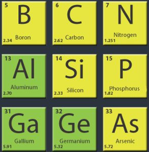
- N-type: Doped with pentavalent atoms (e.g., phosphorus, arsenic). Each dopant atom donates one free electron, making electrons the majority carriers. The Fermi level shifts closer to the conduction band.
- P-type: Doped with trivalent atoms (e.g., boron, gallium). Each dopant accepts an electron, creating a hole as the majority carrier. The Fermi level moves toward the valence band.
While silicon dominates (>95% of all semiconductor devices) due to its abundant raw material (sand), stable native oxide (SiO₂), and mature fabrication infrastructure, other materials serve specialized roles:
- Germanium (Ge): Used in early diodes and transistors; lower bandgap (0.67 eV) enables low-voltage operation but suffers from high leakage current.
- Gallium Arsenide (GaAs): High electron mobility makes it ideal for microwave and optoelectronic devices (LEDs, laser diodes, RF amplifiers).
- Silicon Carbide (SiC) & Gallium Nitride (GaN): Wide-bandgap semiconductors (3.2 eV and 3.4 eV respectively). Operate efficiently at >200°C, withstand breakdown voltages >1000 V, and reduce switching losses by up to 70% compared to silicon. Critical for EV chargers, 5G base stations, and aerospace power systems.
Advanced Materials and Future Trends
The next generation of electronics is being built on wide-bandgap (WBG) semiconductors. SiC and GaN enable:
- Higher switching frequencies → smaller passive components (inductors, capacitors)
- Reduced conduction and switching losses → higher system efficiency
- Operation at extreme temperatures → fewer cooling requirements
- Compact designs → vital for drones, satellites, and portable medical devices
Emerging research focuses on 2D materials (e.g., graphene, MoS₂), organic semiconductors, and quantum dot devices—but for now, SiC and GaN represent the most commercially viable leap forward since the invention of the MOSFET.
🚀? Ready to Dive Deeper
You’ve explored the key concepts, but the full version takes you further into advanced electronics and computer components. Learn the deeper insights and practical applications you won’t find in the free preview.
✨ Inside the full article, you’ll discover:
– Detailed analysis of advanced transistor circuits
– Real-world applications in electronics and computing
– Expert tips and diagrams for better understanding
📘 This article is your next step to mastering modern electronics.
🔥 Download the Full Version Here
For more related insights, read our next transistor article.